4-Bit Counter and Signal Bus Implementation
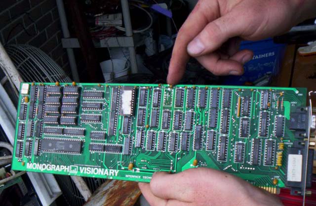
Hardware for the implementation consisted of first finding the components that were required. Some IC chips were salvaged from boards that were simply lying around, and others were purchased.
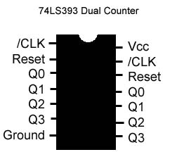
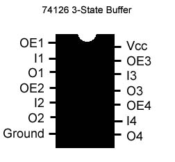
The IC chip found for the 4-Bit Counter is a 74LS393 (it is a dual counter, one single IC chip contains 2 4-Bit Counters), and the IC chip used for the signal bus is a 74126 (it is a 3-state buffer). The following image is the pinout for these two IC chips:
| 74LS393 | |
|---|---|
| Pin | Definition |
| /CLK | /CLK refers to "Clock". The 4-Bit Counter is traditionally used to count clock ticks in a computer. For this application, we use it to count signal pulses. In particular to this IC chip, the leading edges of the pulses are counted. |
| Reset | Reset is responsible for resetting the counter to 0. When a TTL pulse occurs at this pin, while at the HIGH state (+5V), the counter is in "reset mode" and does not store input pulses. |
| Q0-Q3 | These are the output pins. They represent the 4 bits of the binary number of pulses stored. Q0 represents 1, Q1 2, Q2 4, and Q3 8. Since these outputs will be a TTL high or low, representing 1 and 0 repsectively, numbers produced by the output will be between 0 and 15. |
| Ground | The ground connection. |
Note that the 74LS393 IC chip contains two counters, whose pins are on the left and right sides, and they are independent from one another (aside from sharing the same power source). Therefore, only one of these IC chips is needed to count the pulses from two sensor inputs.
| 74126 | |
|---|---|
| Pin | Definition |
| OE | Output Enable. This pin is the mechanism by which one of the inputs is "selected". When this pin receives a TTL 0 (a low voltage), regardless of input, the output pin is "high impedance". This means that it is as if the output is effectively not there - as if the output pin is not connected to anything. |
| I | The input pin. |
| O | Output pin. This IC chip is called a 3-State Buffer because the output is either TTL 0 or 1, or HZ (high impedance). |
Note that for this IC chip, there are actually 4 3-State Buffers. All 4 buffers will be used on this chip, each one for a single bit of the input number given by the 4-Bit Counter. Therefore, one 74126 IC chip is needed for each sensor.
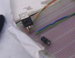
These TTL IC chips require a 5V power supply. One was created using a 750 uF capacitor and a voltage regulator (an image of this setup is below).
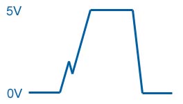
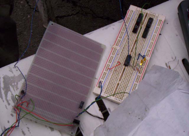
Before soldering the 4-Bit Counter to the prototyping board, a preliminary circuit was made on a breadboard, and some LED's were on the output pins of the 4-Bit Counter (an image of this setup is here). The 4-Bit Counter was connected to the input signal from the Hall Effect Sensor (to be used as a tachometer reading). An irregular pattern was discovered in the periodic flashing of the LED's, and an oscilloscope was used to examine the waveform before the 4-Bit Counter. A break in the voltage wave was discovered after "zooming in" on a portion of the wave. The wave appeared as in the following image (however the perturbation was much less exaggerated):
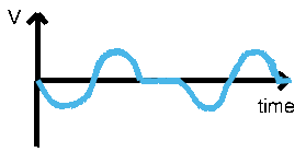
The brief spike in the wave (which was not appearing at a regular interval) was causing the 4-Bit Counter to count an additional pulse because it was occuring within a specific voltage range around TTL 0 that triggers the 4-Bit Counter. Bryan looked into the source of the perturbation extensively, and discovered that the Hall Effect Sensor created a voltage wave that was both negative and positive, as in the following diagram:
This is important because the base connector of the transistor is not built for handling negative voltages. Without entering the technical details of electrical engineering in too much detail - these negative voltages caused a "jitter" due to loading and unloading of current in the transistor components. The circuit diagram for the Hall Effect Sensor signal conditioner module was revised. The revisions are captured in purple in the following diagram:
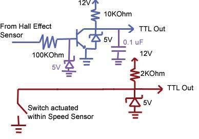
An additonal 5V zener was added prior to the transistor for the purpose of eliminating the negative voltages (strictly voltages between 0-5V get to the transistor, excess voltages pass through the zener to ground). In addition, a 0.1 uF capacitor was added to "smooth out" the voltage wave to TTL Out and eliminate any jitter caused by the transistor that the 4-Bit Counter may pick up as additional pulses.
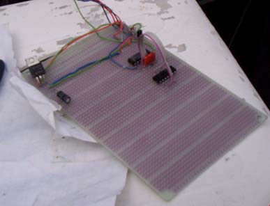
After these changes, we examined the LED's and the intervals between flashes were very regular. We also tested different frequencies of pulse input by revving up the engine and the speed of the LED flashes changed in accord. The next step was transferring the breadboard circuitry onto the prototyping board and soldering it in. This image is of the process partially completed.
In this image, the 4-Bit Counter is fully connected, and the first IC chip for the signal bus has been added. We used a portion of an IDE cable to run the 4 bits of the input signal from chip to chip. By convention, the "red striped" wire of the group is for the smallest bit of the number given by the 4-Bit Counter. The following image is after both bus drivers are connected and installed onto the prototyping board:
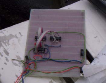
The circuitry is almost complete. All that remains is to merge the outputs from the bus driver IC chips (the 3-State Buffers) and connect to the lines in the parallel port, and connect lines from the parallel port to the 2 Reset pins on the 4-Bit Counters. The following modular diagram conveys this:
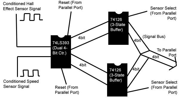
Note that this diagram ignores particular pinouts and Vcc and ground connections. In addition, since the 3-State Buffer IC chips contain 4 buffers each, the OE (Output Enable) for all 4 pins on the IC chip are connected together to a single Sensor Select lead from the parallel port. This is because one 3-State Buffer IC chip contains all 4 bits of signal data for a particular sensor.