The clock is not drawn below;
it should be wired into the clock input of each D flip-flop.
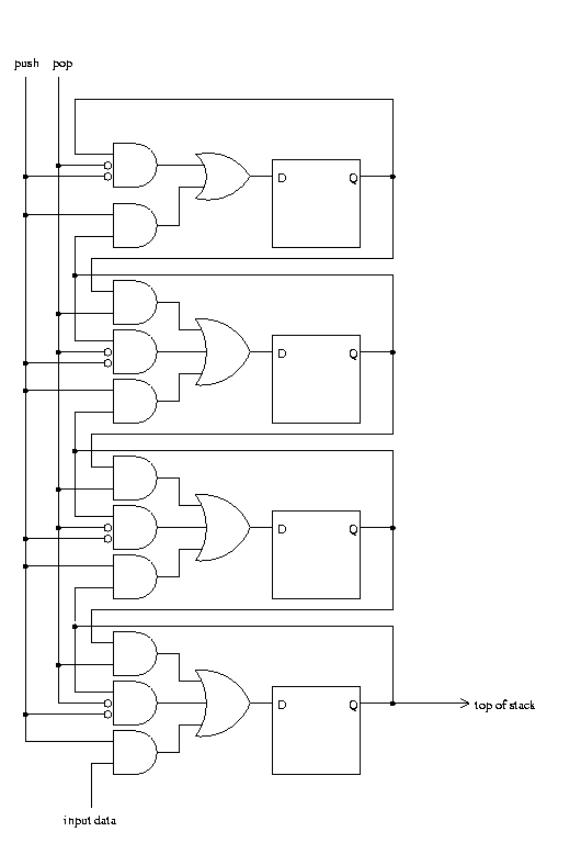
This is almost the same as a shift register.
The 'D' inputs are all either
- the current value, if push and pop are both 0;
- the value from deeper in the stack, if pop is 1; or
- the value from higher in the stack, if push is 1. In this case, the top
D flip-flop gets the input line.
This selection is accomplished by ANDing together each data value with the
control lines which indicate that it should be the one going into the D
flip-flop, and then ORing the results of all these together. In normal
operation, exactly one of the controls will be 1; that AND gate's data will
pass through and the other AND gates will yield 0. ORing these together will
pass through the desired data value.
For further explanation, read up on shift registers.
Note that during a "pop", the bottom of my stack will get zeroed.
This is acceptable because
this is a "don't care" situation, as it is an error to pop values not
pushed.
[sequential circuit problems]
[main course page]