Lab three questions and answers
Here are some notes about lab three (some in Q&A format, some not).
Suggestions for additions to this list are welcome (via e-mail).
Remember that
the list of control signals in each microcode step
is a list of which ones are supposed to be 1 for
that clock cycle, and all other control signals are supposed to be 0.
(This is crucial to understanding what these microcode instructions
mean!)
Q: On the handout, it says that the
IR will determine which function is to be performed by the ALU. So does
that mean that we just arbitrarily assign a code for each function?
A: Yes. Of course there are only two
possibilities. The IR contains the instruction being executed, and since it's
only 1 bit and there is an opcode field, the opcode is that entire one bit.
So either 1 means AND and 0 means XOR, or vice versa.
Q: What does the "decoding" circuitry connected to the IR do?
A: In the case of this simple architecture, nothing.
The IR contents is just one bit and there's nothing interesting to decode
there.
It's all opcode; that one bit goes directly into the ALU to select which
operation is performed.
Q: Must we use a multiplexer to implement the ALU?
A: No, although you can if you like. But I suggest doing it more simply.
Just write out the complete formula for what the ALU calculates, with IR
being one of the variables in your algebraic expression.
Actually, what you'll get is the same as what you'd get if you expanded all
the circuitry for a two-input multiplexer.
But I think you'll find it easier to understand and work with if you do it
all within boolean algebra, by just making formulas involving A, B, and IR.
Q: On the D flip-flop chips 74LS174 and 74LS175, there is only one Clock line.
So I need a separate chip for each register, right?
A: You would indeed, if you were to use those chips for your registers.
I suggest instead using the 74LS74 chip (note number 74 instead of 174!) which
only has two D flip-flops but they are separately-clocked.
Q: Do we use a separate tri-state device for every 'out' control signal?
And if so, does this mean that we can't use the 74LS367A chip?
A: You do indeed use a separate tri-state device for every 'out' control signal.
That means that you only need one data bit for that tri-state device.
The 74LS125 chip is optimal for this purpose. However, there might not be
enough to go around, so it would be best if you were prepared to be able to
use the 74LS367A chip instead. Each 74LS367A chip gives you only two usable
tri-state drivers because you only want one bit of each of the
identically-controlled group of them.
That is, you'll just want to ground or power three of the four data bits
corresponding to
one of the control signals, and one of the two data bits corresponding to
the other control signal.
Q: How do I make a "bus"?
A: Just connect all the wires together.
All the tristated data outputs, and all the D inputs, all get connected
together in a big bundle. That's the bus.
In practice in working with the breadboard you probably want to chain them;
i.e. if A, B, C, D, E, and F are all connected to the bus, you might connect A
to B, and B to C, and C to D, and D to E, and E to F; rather than attempting
to connect all of A, B, C, D, and E to F (for which there aren't enough holes
in that column in the breadboard).
As stated on the lab 3 handout, "the control input of the
tri-state bus drivers used in the lab
means 'output disable' instead of 'output enable'"; so the input should be 0
to turn them on and 1 to turn them off.
But
this doesn't mean you necessarily need any extra circuitry. Because the
tri-state device control lines will be going directly from input switches.
So just consider the input switches to be upside-down, and then you have
achieved the necessary inversion.
Q: What's a timing diagram?
A: A timing diagram plots the logic levels of various items of interest in
your circuit against time.
It shows how values change over time.
There are timing diagrams in a few places in the Hamacher et al textbook.
I suggest particularly looking at those
on pages 686 (section A.5.2, "Propagation Delay")
and 691 (section A.6.1, "Gated Latches").
I've drawn some diagrams somewhat like this in lecture.
There is no CPU clock for you to draw. The items of interest are the control
lines you're flipping the switches of, and probably the contents of some
registers.
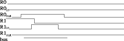
Here's an example for the transfer R1 <- [R0].
We turn on the LOAD line for R1 after turning on the
R0out line, and most of all, it's important to turn off
the LOAD line for R1 before turning off the R0out.
This is illustrated in this figure.
It's "not to scale", obviously. The purpose of this timing diagram,
like those on the above-cited pages of the textbook, isn't
really the timing. It's to show what happens in what order.
I've shown a value for the bus as well.
If you want to do this, you want to use some notation for showing that the bus
is neither powered nor grounded a lot of the time. Here I've simply not drawn
the line. If you want to draw it halfway between a logic 1 and logic 0, that
would be reasonable, too, if you can make it clear.
[all CSC 258 labs]
[main course page]